PCB process (printed circuit board process) is the backbone of modern electronics. It helps connect various electric connections among components like resistors, capacitors, transistors, diodes, etc. It has a printed pathway by which electricity flows through these components. That’s how it fulfills your device’s electric circuit requirement and brings it to life.
From simplest gadgets like digital watches and calculators to complex ones like computers and smartphones, PCBs are used in them. So, manufacturers, designers, and engineers must understand the PCB process and its manufacturing.
This article will guide you in understanding how it is manufactured step by step. Let’s dive into it.
Step-by-step Breakdown of PCB Process Manufacturing
The number of steps in the manufacturing process depends on how many layers the PCB has. A PCB can be single-layer, double-layer, or multilayered. The more layers a PCB has, the more steps are required.
Here are the main steps:
- PCB Design
The first step in the PCB process is to design it using software like Extended Gerber, KiCAD, or Altium. The design helps manufacturers to get the exact pathway of components, wiring, and electricity.
The design is sent for printing after converting into Gerber files and checked by a fabricator, DFM (Design for Manufacture), which confirms that the design satisfies all minimum requirements for manufacturing. - Printing the PCB Design
A printer named Plotter printer prints PCB design. Two types of inks are used. Black ink indicates conductive copper and PCB circuits. Clear ink shows non-conductive parts like fiberglass (substrate).
At first, the copper layer is coated on the substrate(FR4) from both sides. Then, a photomask is laminated over this copper layer. - Removing Unwanted Copper
This step includes applying a photoresist to the copper board before exposing it to UV light through a photomask. After that, the board is immersed in a chemical solution that removes unhardened photoresist and unwanted copper. This step is also called etching. - Drilling and Plating
Geber files have a map for drilling holes. So, holes are drilled to place components, and then conductive material (copper) is plated in holes to create connections between components and other PCB layers. - Solder Mask Application
The PCB panel is first cleaned before applying epoxy solder mask ink. Then, the board undergoes a UV blast, which passes through the solder mask film. Some covered areas will be unhardened and removed afterward. - Surface Finishing
In this step, finishes like Electroless nickel immersion gold(ENIG), Hot air solder leveling (HASL), and immersion silver are applied to printed circuit boards to fend off oxidation and enhance solderability. - Silkscreen Layer
Silksreening includes printing logos, symbols of components, and reference points. It assists in recognizing components during placement and assembly. - Assembly
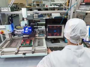
In Assembly, components can be placed and soldered through any of these technologies:
●SMT( Surface mount technology): It is a process in which components are directly mounted on the surface of PCB.
●Through-Hole Technology: In this process, components are inserted through holes drilled in the board. - Testing and Quality Control
This final testing and quality control step is performed before packaging and shipping. It ensures that the PCB meets the design requirement and has the same hole size on all layers. If any board fails in automated optical inspection (AOI), It undergoes repairing and retesting.
Conclusion
Understanding the PCB process is crucial for those involved in its manufacturing or design. In today’s age, the demand for electronic devices is continuously increasing, and so is the demand for PCBs. Therefore, learning the steps of PCB manufacturing properly to produce high-quality boards is significant.
0