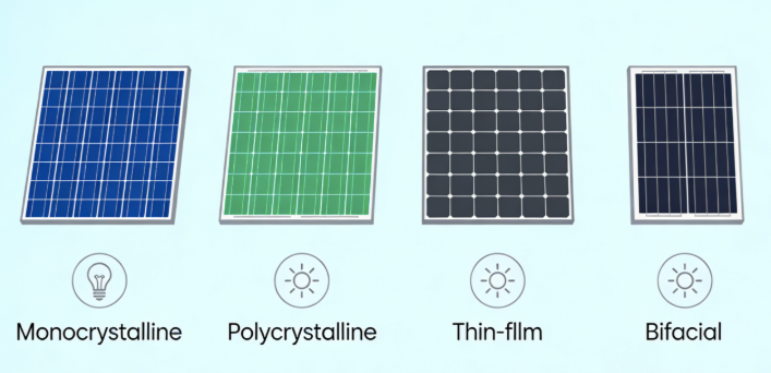
In solar photovoltaic manufacturing, both N-type and P-type monocrystalline silicon wafers are widely used, and understanding their differences is essential for technology selection. A p type silicon wafer has long dominated the market due to its mature process and cost advantages, while N-type wafers have gained attention for their higher efficiency and lower degradation. The following sections focus on the main differences between N-type and P-type silicon wafers in solar applications.

1. Doping and Material Structure Differences
- N-Type vs P-Type Doping
The primary difference lies in doping materials. A p type silicon wafer is doped with boron, creating holes as the main charge carriers. In contrast, N-type silicon wafers use phosphorus doping, where electrons become the dominant carriers.
- Impact on Carrier Behavior
Because electrons move faster than holes, N-type wafers generally show better carrier transport performance, while the p type silicon wafer offers stable electrical behavior based on its mature structure.
2. Conversion Efficiency Differences
- Efficiency Potential Comparison
N-type solar cells typically achieve higher conversion efficiency than cells based on a p type silicon wafer, mainly due to lower recombination losses.
- Practical Performance Gap
However, with continuous improvements in cell design, the efficiency gap between N-type and p type silicon wafer technologies has narrowed in many commercial applications.
3. Degradation Characteristics Differences
- Light-Induced Degradation
A known limitation of the p type silicon wafer is light-induced degradation (LID), caused by boron-oxygen complexes. N-type wafers largely avoid this issue.
- Long-Term Output Stability
Although N-type wafers perform better in this aspect, modern processing methods help p type silicon wafer modules maintain stable long-term output after initial degradation.
4. Manufacturing Cost Differences
- Production Cost Comparison
A key advantage of the p type silicon wafer is its lower production cost, supported by highly standardized and large-scale manufacturing systems.
- Equipment and Process Compatibility
N-type wafer production often requires upgraded equipment, while p type silicon wafer manufacturing remains more cost-efficient for existing production lines.
5. Application and Market Position Differences
- Typical Use Cases
The p type silicon wafer is widely applied in cost-sensitive utility-scale projects, whereas N-type wafers are commonly used in high-efficiency or premium solar modules.
- Selection Strategy
This difference reflects a trade-off between performance and investment, where p type silicon wafer solutions remain competitive in mainstream markets.
Conclusion
Overall, the main differences between N-type and p type silicon wafer technologies include doping method, efficiency potential, degradation behavior, and manufacturing cost. While N-type wafers offer higher performance and lower degradation, the p type silicon wafer continues to play a vital role in the solar photovoltaic industry due to its maturity, reliability, and economic advantages.
0