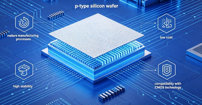
The p-type silicon wafer is one of the most widely used foundational materials in semiconductor device manufacturing. It plays a crucial role in producing integrated circuits, diodes, transistors, and photovoltaic cells. By introducing boron as a dopant into high-purity silicon, p-type wafers create “holes” as the primary charge carriers, enabling stable and controlled electrical conductivity. Compared with other wafer types, the p-type silicon wafer is valued for its cost efficiency, mature manufacturing process, and reliable performance across a wide range of electronic applications. These advantages make it a preferred choice in both mass production and industrial-scale semiconductor fabrication.
Mature Manufacturing Process and Stable Production Quality
One of the most significant advantages of the p-type silicon wafer is its highly developed and stable production process.
- Well-established industrial technology: P-type wafers have been used for decades, resulting in highly refined manufacturing techniques that ensure consistent quality output.
- High production yield: The mature doping process with boron allows manufacturers to achieve stable electrical properties with minimal defects.
- Process compatibility: P-type wafers are compatible with a wide range of semiconductor fabrication steps, including oxidation, diffusion, and etching.
- Reduced production risk: Due to its long-standing industrial use, production processes are well understood, reducing uncertainty during mass manufacturing.
This maturity makes p-type wafers highly reliable for large-scale semiconductor production.
Cost Efficiency and Large-Scale Applicability
Another major benefit of the p-type silicon wafer is its cost advantage, especially in high-volume production environments.
- Lower raw material cost: The doping materials and production steps used for p-type wafers are generally less expensive compared to n-type alternatives.
- Economies of scale: Because p-type wafers are widely used, manufacturers benefit from large-scale production efficiency, reducing unit costs.
- Simplified processing requirements: The fabrication process is less complex, which helps reduce energy consumption and operational expenses.
- Ideal for mass-market devices: Many consumer electronics and standard photovoltaic panels rely on p-type wafers due to their affordability.
This cost-effectiveness makes p-type wafers highly attractive for commercial semiconductor production.
Reliable Electrical Performance in Standard Applications
The p-type silicon wafer provides stable and predictable electrical characteristics, making it suitable for a wide range of applications.
- Stable hole-based conductivity: The presence of positive charge carriers ensures consistent current flow under normal operating conditions.
- Good thermal stability: P-type wafers perform reliably across moderate temperature variations, making them suitable for everyday electronic devices.
- Balanced electrical behavior: They offer a good balance between conductivity and control, which is essential for circuit design.
- Compatibility with CMOS technology: P-type substrates are widely used in complementary metal-oxide-semiconductor (CMOS) structures.
These electrical properties ensure dependable performance in most conventional semiconductor applications.
Wide Application in Semiconductor and Solar Industries
The versatility of the p-type silicon wafer allows it to be used across multiple industries.
- Integrated circuit manufacturing: P-type wafers serve as foundational substrates in many chip designs used in computers and mobile devices.
- Photovoltaic solar cells: They are commonly used in traditional solar panels due to their cost efficiency and reliable performance.
- Discrete semiconductor devices: Components such as diodes and transistors often rely on p-type silicon structures.
- Industrial electronics systems: Power management devices and control systems frequently utilize p-type wafer-based components.
This broad applicability reinforces its importance in modern technology ecosystems.
Compatibility with Advanced Fabrication Processes
Although considered a traditional material, the p-type silicon wafer remains highly compatible with modern semiconductor technologies.
- Integration with n-type regions: It is commonly combined with n-type materials to form p-n junctions, which are essential in most semiconductor devices.
- Adaptability to modern lithography: P-type wafers can be used in advanced patterning and microfabrication processes.
- Scalability for miniaturization: They support the production of increasingly smaller and more efficient electronic components.
- Flexible device architecture design: Engineers can design complex circuit structures using p-type substrates without major process limitations.
This compatibility ensures that p-type wafers remain relevant even as semiconductor technology continues to evolve.
Conclusion
The p-type silicon wafer offers several key advantages, including mature manufacturing processes, cost efficiency, stable electrical performance, wide industrial applicability, and strong compatibility with modern fabrication technologies. These strengths make it a fundamental material in semiconductor device production, particularly for large-scale and cost-sensitive applications. While newer materials and n-type wafers are gaining traction in high-performance sectors, p-type wafers continue to play an essential role in powering everyday electronics and renewable energy systems.
0